+353-1-416-8900REST OF WORLD
+44-20-3973-8888REST OF WORLD
1-917-300-0470EAST COAST U.S
1-800-526-8630U.S. (TOLL FREE)
New

E-Beam Wafer Inspection Systems - Global Strategic Business Report

  • PDF Icon

    Report

  • 258 Pages
  • January 2025
  • Region: Global
  • Global Industry Analysts, Inc
  • ID: 4804752
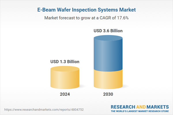
The global market for E-Beam Wafer Inspection Systems was estimated at US$1.1 Billion in 2023 and is projected to reach US$3.6 Billion by 2030, growing at a CAGR of 17.7% from 2023 to 2030. This comprehensive report provides an in-depth analysis of market trends, drivers, and forecasts, helping you make informed business decisions.

Global E-Beam Wafer Inspection Systems Market - Key Trends & Drivers Summarized

What Are E-Beam Wafer Inspection Systems?

E-Beam (Electron Beam) wafer inspection systems are advanced tools used in the semiconductor manufacturing industry to detect and analyze defects on wafers at a nanometric scale. These systems utilize electron beams to scan the surface of semiconductor wafers, providing high-resolution images and detailed information about potential defects. E-Beam inspection is crucial for ensuring the quality and reliability of semiconductor devices, as it can identify minute defects that might impact the performance and yield of integrated circuits. The precision and accuracy of E-Beam inspection systems make them indispensable in the production of advanced semiconductor technologies.

How Are Industry Demands Shaping This Market?

The demands of the semiconductor industry are significantly shaping the market for E-Beam wafer inspection systems. As semiconductor devices become increasingly complex and miniaturized, the need for more precise and accurate inspection tools is growing. The transition to smaller node sizes and the development of advanced technologies such as 3D NAND, FinFET, and multi-patterning require inspection systems that can detect even the smallest defects. The push for higher yield and reliability in semiconductor manufacturing is driving the adoption of E-Beam inspection systems, which offer the resolution and sensitivity needed to meet these stringent requirements.

What Technological Innovations Are Influencing This Field?

Technological innovations are at the forefront of advancements in E-Beam wafer inspection systems. Improvements in electron optics, detector sensitivity, and data processing algorithms are enhancing the performance and efficiency of these systems. The integration of artificial intelligence and machine learning is enabling more sophisticated defect detection and classification, reducing false positives and improving inspection throughput. Additionally, the development of hybrid inspection systems that combine E-Beam with optical inspection technologies is providing a more comprehensive solution for defect analysis. These innovations are essential for addressing the challenges of inspecting advanced semiconductor nodes and ensuring the production of high-quality devices.

What Factors Are Driving Market Growth?

The growth in the E-Beam wafer inspection systems market is driven by several factors, including the increasing complexity of semiconductor devices, the need for higher yield and reliability, and technological advancements in inspection tools. The ongoing development of smaller and more complex semiconductor nodes is creating a demand for more precise and accurate inspection systems. The push for higher yield and lower defect rates in semiconductor manufacturing is also driving market growth, as manufacturers seek to optimize production and reduce costs.

Technological advancements in electron optics, AI, and data processing are enhancing the capabilities of E-Beam inspection systems, making them more effective and efficient. Additionally, the expansion of the semiconductor industry, driven by the growing demand for electronics and emerging technologies such as 5G, IoT, and AI, is further propelling the market for E-Beam wafer inspection systems.

Key Insights:

  • Market Growth: Understand the significant growth trajectory of the Defect Imaging Application segment, which is expected to reach US$1.4 Billion by 2030 with a CAGR of a 18.0%. The Lithographic Qualification Application segment is also set to grow at 19.6% CAGR over the analysis period.
  • Regional Analysis: Gain insights into the U.S. market, estimated at $139.8 Million in 2023, and China, forecasted to grow at an impressive 21.5% CAGR to reach $931.3 Million by 2030. Discover growth trends in other key regions, including Japan, Canada, Germany, and the Asia-Pacific.

Why You Should Buy This Report:

  • Detailed Market Analysis: Access a thorough analysis of the Global E-Beam Wafer Inspection Systems Market, covering all major geographic regions and market segments.
  • Competitive Insights: Get an overview of the competitive landscape, including the market presence of major players across different geographies.
  • Future Trends and Drivers: Understand the key trends and drivers shaping the future of the Global E-Beam Wafer Inspection Systems Market.
  • Actionable Insights: Benefit from actionable insights that can help you identify new revenue opportunities and make strategic business decisions.

Key Questions Answered:

  • How is the Global E-Beam Wafer Inspection Systems Market expected to evolve by 2030?
  • What are the main drivers and restraints affecting the market?
  • Which market segments will grow the most over the forecast period?
  • How will market shares for different regions and segments change by 2030?
  • Who are the leading players in the market, and what are their prospects?

Report Features:

  • Comprehensive Market Data: Independent analysis of annual sales and market forecasts in US$ Million from 2023 to 2030.
  • In-Depth Regional Analysis: Detailed insights into key markets, including the U.S., China, Japan, Canada, Europe, Asia-Pacific, Latin America, Middle East, and Africa.
  • Company Profiles: Coverage of major players in the Global E-Beam Wafer Inspection Systems Market such as Aerotech, Inc., Applied Materials, Inc., ASML Holding NV, Hitachi High-Technologies Corporation, Holon Co, Ltd. and more.
  • Complimentary Updates: Receive free report updates for one year to keep you informed of the latest market developments.

Some of the 18 companies featured in this Global E-Beam Wafer Inspection Systems market report include:

  • Aerotech, Inc.
  • Applied Materials, Inc.
  • ASML Holding NV
  • Hitachi High-Technologies Corporation
  • Holon Co, Ltd.
  • KLA Corporation
  • MKS Instruments, Inc.
  • PDF Solutions
  • Photo electron Soul Inc.

Table of Contents

I. METHODOLOGYII. EXECUTIVE SUMMARY
1. MARKET OVERVIEW
  • As Digitalization Transforms Every Aspect of Modern Life, Semiconductors Emerge as the Most Sought-After Commodity
  • The Semiconductor Decade is on its Way Guided by the Digitalization Wave: Digital Transformation (DX) Spending of Business Practices, Products & Organization (In US$ Billion) for Years 2021 Through 2025
  • Digital Transformation Across Industries Shape a Robust Semiconductor Industry Vital to the Continued Evolution of Human Civilization: Global Semiconductor Revenue Share Breakdown by End-Use for 2024E
  • Inside the World of Semiconductor Manufacturing: A Quick Dive
  • Salient Forces Shaping the Future Trajectory of Global Semiconductor Industry
  • Why Is Wafer Inspection So Important in Semiconductor Manufacturing?
  • E-Beam Wafer Inspection System: Definition & Technology Overview
  • Optical Vs E-Beam Wafer Inspection System
  • In-Line Wafer Inspection Technology: A Review
  • Advanced EBI Systems for Massive Metrology Over Wider Inspection Areas
  • Economic Frontiers: Trends, Trials & Transformations
  • In a World Torn by Geopolitical Instability & War, Steadfastness of Global GDP Becomes Increasingly Unpredictable Given the Many Direct and Indirect Economic Repercussions: World Economic Growth Projections (Real Gross Domestic Product (GDP), Annual % Change) for the Years 2022 Through 2025
  • All Eyes on Global Inflation, the Main Risk Factor in Global Markets: Global Headline Inflation Rates (In %) for the Years 2019 through 2025
  • With Oil Prices Influencing the Rate of inflation, it Remains the Most Watched Commodity in Global Markets: Global Average Annual Brent Crude Oil Price (In US$ Per Barrel) for Years 2019 through 2025
  • Semiconductor Industry: Implications of Emerging Trends & Developments for E-Beam Wafer Inspection Systems
  • Global Market Outlook
  • Less Than 1 nm Systems to Witness Rapid Growth
  • Asia-Pacific Continues to Boost Market Prospects
  • Competition
  • E-Beam Wafer Inspection Systems - Global Key Competitors Percentage Market Share in 2024 (E)
  • Competitive Market Presence - Strong/Active/Niche/Trivial for Players Worldwide in 2024 (E)
  • Recent Market Activity
  • Influencer/Product/Technology Insights
2. FOCUS ON SELECT PLAYERS
3. MARKET TRENDS & DRIVERS
  • Here’s How Dynamics of E-Beam Wafer Inspection Systems Is Tied to Semiconductor Manufacturing
  • Growing Demand for Advanced Node Semiconductor Manufacturing Propels Need for Wafer Inspections, Spurring Market Opportunities
  • Wafer Production Moves to Next Level with Innovations in Imaging-based Inspection Systems
  • Wafer Production Moves to Next Level with Innovations in Imaging-based Inspection Systems
  • Growing Prominence of Automated Wafer Inspection in Semiconductor Manufacturing
  • How Do Automated Wafer Inspection Systems Fare Over Traditional Systems
  • With Digitalization Equaling Survival and Wafers as the Heart of Electronics Continuing to Grow in Demand, Wafer Inspection Poised to Make Significant Strides
  • This is How Wafers Are Beginning to Hog the Limelight
  • Migrating from Horse Power to Chip Power, Automotive Industry Steps Up Reliance on Semiconductor Chips & ICs: Automotive Electronics as a % of Total Vehicle Cost for Years 2000, 2010, 2020 and 2030
  • Expanding IoT Ecosystem Steps Up Reliance on Semiconductor Chips & ICs: Global IoT Connections (In Billion) for Years 2024, 2026, 2028 and 2030
  • Robust Renewed Spending on Industrial & Manufacturing Automation Spurs Demand for Industrial Electronics, Present Opportunities for Wafer Inspection Market: Global Market for Industrial Semiconductors (In US$ Billion) for Years 2020, 2022 & 2024
  • Ramping Up of Infrastructure in Datacenters, the Starting Point for Successful Digital Transformation, Drives Demand for Semiconductor Products & Solutions
  • Rising Demand for Datacenter Hardware Drives Demand Growth for Semiconductors: Global Datacenter Infrastructure Market (In US$ Billion) for Years 2020, 2022, and 2024
  • Focus on Easing Chip Shortage and Subsequent Investments to Expand Production Capacity Boost Semiconductor Manufacturing Equipment Market, Driving Market Gains
  • Annual Global IC Wafer Capacity (in Millions of Wafers per Year) for 2015 through 2025P
  • Market to Benefit from the Higher Challenges Involved In Inspecting Reclaimed Wafers
  • Growing Use of Reclaimed Silicon Wafers Steps Ups the Onus of Quality Control & Inspection Technologies: Global Opportunity in Silicon Reclaimed Wafers (In US$ Million) for Years 2021, 2023, 2025 & 2027
  • Multi-Beam Inspection Technology Rises in Prominence & In Revenue Potential
  • Increasing Role of EUV Lithography in Semiconductor Manufacturing Fuels Need for Advanced E-Beam Wafer Inspection
  • How Is the Integration of AI and ML Transforming E-Beam Wafer Inspection Systems?
  • Rise of Smart E-Beam for Defect Identification & Analysis in the Nanoscale Technology Nodes
  • Pushing the Limits: The Next Frontier in Wafer and Package Defect Inspection
  • Revolutionizing Chip Quality with Next-Gen E-Beam Inspection
  • Advanced Imaging Techniques for Semiconductor Wafer Inspection: Vital Role of E-Beam Inspection Systems
  • Why Hybrid Inspection Systems Are Game-Changing?
  • E-Beam Inspection Technology Poised to Gain Prominence in High-Volume Semiconductor Manufacturing
  • Continued Technology Innovation Remains Crucial for Future Growth
  • Investments in Traditional Technology Nodes on the Rise, MB Writers and MPC Solutions Register Growing Adoption
  • Major Challenges Facing the E-Beam Wafer Inspection Systems Market
  • Speed: A Significant Bottleneck for E-Beam Wafer Inspection Systems
4. GLOBAL MARKET PERSPECTIVE
  • Table 1: World Recent Past, Current & Future Analysis for More Than 10 Nm Size by Geographic Region - USA, Canada, Japan, China, Europe, Asia-Pacific and Rest of World Markets - Independent Analysis of Annual Revenues in US$ Thousand for Years 2023 through 2030 and % CAGR
  • Table 2: World 7-Year Perspective for More Than 10 Nm Size by Geographic Region - Percentage Breakdown of Value Revenues for USA, Canada, Japan, China, Europe, Asia-Pacific and Rest of World for Years 2024 & 2030
  • Table 3: World Recent Past, Current & Future Analysis for 1 To 10 Nm Size by Geographic Region - USA, Canada, Japan, China, Europe, Asia-Pacific and Rest of World Markets - Independent Analysis of Annual Revenues in US$ Thousand for Years 2023 through 2030 and % CAGR
  • Table 4: World 7-Year Perspective for 1 To 10 Nm Size by Geographic Region - Percentage Breakdown of Value Revenues for USA, Canada, Japan, China, Europe, Asia-Pacific and Rest of World for Years 2024 & 2030
  • Table 5: World Recent Past, Current & Future Analysis for Less Than 1 Nm Size by Geographic Region - USA, Canada, Japan, China, Europe, Asia-Pacific and Rest of World Markets - Independent Analysis of Annual Revenues in US$ Thousand for Years 2023 through 2030 and % CAGR
  • Table 6: World 7-Year Perspective for Less Than 1 Nm Size by Geographic Region - Percentage Breakdown of Value Revenues for USA, Canada, Japan, China, Europe, Asia-Pacific and Rest of World for Years 2024 & 2030
  • Table 7: World Recent Past, Current & Future Analysis for Defect Imaging Application by Geographic Region - USA, Canada, Japan, China, Europe, Asia-Pacific and Rest of World Markets - Independent Analysis of Annual Revenues in US$ Thousand for Years 2023 through 2030 and % CAGR
  • Table 8: World 7-Year Perspective for Defect Imaging Application by Geographic Region - Percentage Breakdown of Value Revenues for USA, Canada, Japan, China, Europe, Asia-Pacific and Rest of World for Years 2024 & 2030
  • Table 9: World Recent Past, Current & Future Analysis for Lithographic Qualification Application by Geographic Region - USA, Canada, Japan, China, Europe, Asia-Pacific and Rest of World Markets - Independent Analysis of Annual Revenues in US$ Thousand for Years 2023 through 2030 and % CAGR
  • Table 10: World 7-Year Perspective for Lithographic Qualification Application by Geographic Region - Percentage Breakdown of Value Revenues for USA, Canada, Japan, China, Europe, Asia-Pacific and Rest of World for Years 2024 & 2030
  • Table 11: World Recent Past, Current & Future Analysis for Bare Wafer OQC / IQC Application by Geographic Region - USA, Canada, Japan, China, Europe, Asia-Pacific and Rest of World Markets - Independent Analysis of Annual Revenues in US$ Thousand for Years 2023 through 2030 and % CAGR
  • Table 12: World 7-Year Perspective for Bare Wafer OQC / IQC Application by Geographic Region - Percentage Breakdown of Value Revenues for USA, Canada, Japan, China, Europe, Asia-Pacific and Rest of World for Years 2024 & 2030
  • Table 13: World Recent Past, Current & Future Analysis for Wafer Dispositioning Application by Geographic Region - USA, Canada, Japan, China, Europe, Asia-Pacific and Rest of World Markets - Independent Analysis of Annual Revenues in US$ Thousand for Years 2023 through 2030 and % CAGR
  • Table 14: World 7-Year Perspective for Wafer Dispositioning Application by Geographic Region - Percentage Breakdown of Value Revenues for USA, Canada, Japan, China, Europe, Asia-Pacific and Rest of World for Years 2024 & 2030
  • Table 15: World Recent Past, Current & Future Analysis for Reticle Quality Inspection Application by Geographic Region - USA, Canada, Japan, China, Europe, Asia-Pacific and Rest of World Markets - Independent Analysis of Annual Revenues in US$ Thousand for Years 2023 through 2030 and % CAGR
  • Table 16: World 7-Year Perspective for Reticle Quality Inspection Application by Geographic Region - Percentage Breakdown of Value Revenues for USA, Canada, Japan, China, Europe, Asia-Pacific and Rest of World for Years 2024 & 2030
  • Table 17: World Recent Past, Current & Future Analysis for Other Applications by Geographic Region - USA, Canada, Japan, China, Europe, Asia-Pacific and Rest of World Markets - Independent Analysis of Annual Revenues in US$ Thousand for Years 2023 through 2030 and % CAGR
  • Table 18: World 7-Year Perspective for Other Applications by Geographic Region - Percentage Breakdown of Value Revenues for USA, Canada, Japan, China, Europe, Asia-Pacific and Rest of World for Years 2024 & 2030
  • Table 19: World E-Beam Wafer Inspection Systems Market Analysis of Annual Sales in US$ Thousand for Years 2023 through 2030
  • Table 20: World Recent Past, Current & Future Analysis for E-Beam Wafer Inspection Systems by Geographic Region - USA, Canada, Japan, China, Europe, Asia-Pacific and Rest of World Markets - Independent Analysis of Annual Revenues in US$ Thousand for Years 2023 through 2030 and % CAGR
  • Table 21: World 7-Year Perspective for E-Beam Wafer Inspection Systems by Geographic Region - Percentage Breakdown of Value Revenues for USA, Canada, Japan, China, Europe, Asia-Pacific and Rest of World Markets for Years 2024 & 2030
III. MARKET ANALYSIS
UNITED STATES
  • E-Beam Wafer Inspection Systems Market Presence - Strong/Active/Niche/Trivial - Key Competitors in the United States for 2024 (E)
  • Table 22: USA Recent Past, Current & Future Analysis for E-Beam Wafer Inspection Systems by Type - More Than 10 Nm Size, 1 To 10 Nm Size and Less Than 1 Nm Size - Independent Analysis of Annual Revenues in US$ Thousand for the Years 2023 through 2030 and % CAGR
  • Table 23: USA 7-Year Perspective for E-Beam Wafer Inspection Systems by Type - Percentage Breakdown of Value Revenues for More Than 10 Nm Size, 1 To 10 Nm Size and Less Than 1 Nm Size for the Years 2024 & 2030
  • Table 24: USA Recent Past, Current & Future Analysis for E-Beam Wafer Inspection Systems by Application - Defect Imaging Application, Lithographic Qualification Application, Bare Wafer OQC / IQC Application, Wafer Dispositioning Application, Reticle Quality Inspection Application and Other Applications - Independent Analysis of Annual Revenues in US$ Thousand for the Years 2023 through 2030 and % CAGR
  • Table 25: USA 7-Year Perspective for E-Beam Wafer Inspection Systems by Application - Percentage Breakdown of Value Revenues for Defect Imaging Application, Lithographic Qualification Application, Bare Wafer OQC / IQC Application, Wafer Dispositioning Application, Reticle Quality Inspection Application and Other Applications for the Years 2024 & 2030
CANADA
  • Table 26: Canada Recent Past, Current & Future Analysis for E-Beam Wafer Inspection Systems by Type - More Than 10 Nm Size, 1 To 10 Nm Size and Less Than 1 Nm Size - Independent Analysis of Annual Revenues in US$ Thousand for the Years 2023 through 2030 and % CAGR
  • Table 27: Canada 7-Year Perspective for E-Beam Wafer Inspection Systems by Type - Percentage Breakdown of Value Revenues for More Than 10 Nm Size, 1 To 10 Nm Size and Less Than 1 Nm Size for the Years 2024 & 2030
  • Table 28: Canada Recent Past, Current & Future Analysis for E-Beam Wafer Inspection Systems by Application - Defect Imaging Application, Lithographic Qualification Application, Bare Wafer OQC / IQC Application, Wafer Dispositioning Application, Reticle Quality Inspection Application and Other Applications - Independent Analysis of Annual Revenues in US$ Thousand for the Years 2023 through 2030 and % CAGR
  • Table 29: Canada 7-Year Perspective for E-Beam Wafer Inspection Systems by Application - Percentage Breakdown of Value Revenues for Defect Imaging Application, Lithographic Qualification Application, Bare Wafer OQC / IQC Application, Wafer Dispositioning Application, Reticle Quality Inspection Application and Other Applications for the Years 2024 & 2030
JAPAN
  • E-Beam Wafer Inspection Systems Market Presence - Strong/Active/Niche/Trivial - Key Competitors in Japan for 2024 (E)
  • Table 30: Japan Recent Past, Current & Future Analysis for E-Beam Wafer Inspection Systems by Type - More Than 10 Nm Size, 1 To 10 Nm Size and Less Than 1 Nm Size - Independent Analysis of Annual Revenues in US$ Thousand for the Years 2023 through 2030 and % CAGR
  • Table 31: Japan 7-Year Perspective for E-Beam Wafer Inspection Systems by Type - Percentage Breakdown of Value Revenues for More Than 10 Nm Size, 1 To 10 Nm Size and Less Than 1 Nm Size for the Years 2024 & 2030
  • Table 32: Japan Recent Past, Current & Future Analysis for E-Beam Wafer Inspection Systems by Application - Defect Imaging Application, Lithographic Qualification Application, Bare Wafer OQC / IQC Application, Wafer Dispositioning Application, Reticle Quality Inspection Application and Other Applications - Independent Analysis of Annual Revenues in US$ Thousand for the Years 2023 through 2030 and % CAGR
  • Table 33: Japan 7-Year Perspective for E-Beam Wafer Inspection Systems by Application - Percentage Breakdown of Value Revenues for Defect Imaging Application, Lithographic Qualification Application, Bare Wafer OQC / IQC Application, Wafer Dispositioning Application, Reticle Quality Inspection Application and Other Applications for the Years 2024 & 2030
CHINA
  • Market Overview
  • Table 34: China Recent Past, Current & Future Analysis for E-Beam Wafer Inspection Systems by Type - More Than 10 Nm Size, 1 To 10 Nm Size and Less Than 1 Nm Size - Independent Analysis of Annual Revenues in US$ Thousand for the Years 2023 through 2030 and % CAGR
  • Table 35: China 7-Year Perspective for E-Beam Wafer Inspection Systems by Type - Percentage Breakdown of Value Revenues for More Than 10 Nm Size, 1 To 10 Nm Size and Less Than 1 Nm Size for the Years 2024 & 2030
  • Table 36: China Recent Past, Current & Future Analysis for E-Beam Wafer Inspection Systems by Application - Defect Imaging Application, Lithographic Qualification Application, Bare Wafer OQC / IQC Application, Wafer Dispositioning Application, Reticle Quality Inspection Application and Other Applications - Independent Analysis of Annual Revenues in US$ Thousand for the Years 2023 through 2030 and % CAGR
  • Table 37: China 7-Year Perspective for E-Beam Wafer Inspection Systems by Application - Percentage Breakdown of Value Revenues for Defect Imaging Application, Lithographic Qualification Application, Bare Wafer OQC / IQC Application, Wafer Dispositioning Application, Reticle Quality Inspection Application and Other Applications for the Years 2024 & 2030
EUROPE
  • Table 38: Europe Recent Past, Current & Future Analysis for E-Beam Wafer Inspection Systems by Type - More Than 10 Nm Size, 1 To 10 Nm Size and Less Than 1 Nm Size - Independent Analysis of Annual Revenues in US$ Thousand for the Years 2023 through 2030 and % CAGR
  • Table 39: Europe 7-Year Perspective for E-Beam Wafer Inspection Systems by Type - Percentage Breakdown of Value Revenues for More Than 10 Nm Size, 1 To 10 Nm Size and Less Than 1 Nm Size for the Years 2024 & 2030
  • Table 40: Europe Recent Past, Current & Future Analysis for E-Beam Wafer Inspection Systems by Application - Defect Imaging Application, Lithographic Qualification Application, Bare Wafer OQC / IQC Application, Wafer Dispositioning Application, Reticle Quality Inspection Application and Other Applications - Independent Analysis of Annual Revenues in US$ Thousand for the Years 2023 through 2030 and % CAGR
  • Table 41: Europe 7-Year Perspective for E-Beam Wafer Inspection Systems by Application - Percentage Breakdown of Value Revenues for Defect Imaging Application, Lithographic Qualification Application, Bare Wafer OQC / IQC Application, Wafer Dispositioning Application, Reticle Quality Inspection Application and Other Applications for the Years 2024 & 2030
  • Table 42: Europe Recent Past, Current & Future Analysis for E-Beam Wafer Inspection Systems by Geographic Region - France, Germany, Italy, UK and Rest of Europe Markets - Independent Analysis of Annual Revenues in US$ Thousand for Years 2023 through 2030 and % CAGR
  • Table 43: Europe 7-Year Perspective for E-Beam Wafer Inspection Systems by Geographic Region - Percentage Breakdown of Value Revenues for France, Germany, Italy, UK and Rest of Europe Markets for Years 2024 & 2030
FRANCE
  • Table 44: France Recent Past, Current & Future Analysis for E-Beam Wafer Inspection Systems by Type - More Than 10 Nm Size, 1 To 10 Nm Size and Less Than 1 Nm Size - Independent Analysis of Annual Revenues in US$ Thousand for the Years 2023 through 2030 and % CAGR
  • Table 45: France 7-Year Perspective for E-Beam Wafer Inspection Systems by Type - Percentage Breakdown of Value Revenues for More Than 10 Nm Size, 1 To 10 Nm Size and Less Than 1 Nm Size for the Years 2024 & 2030
  • Table 46: France Recent Past, Current & Future Analysis for E-Beam Wafer Inspection Systems by Application - Defect Imaging Application, Lithographic Qualification Application, Bare Wafer OQC / IQC Application, Wafer Dispositioning Application, Reticle Quality Inspection Application and Other Applications - Independent Analysis of Annual Revenues in US$ Thousand for the Years 2023 through 2030 and % CAGR
  • Table 47: France 7-Year Perspective for E-Beam Wafer Inspection Systems by Application - Percentage Breakdown of Value Revenues for Defect Imaging Application, Lithographic Qualification Application, Bare Wafer OQC / IQC Application, Wafer Dispositioning Application, Reticle Quality Inspection Application and Other Applications for the Years 2024 & 2030
GERMANY
  • Table 48: Germany Recent Past, Current & Future Analysis for E-Beam Wafer Inspection Systems by Type - More Than 10 Nm Size, 1 To 10 Nm Size and Less Than 1 Nm Size - Independent Analysis of Annual Revenues in US$ Thousand for the Years 2023 through 2030 and % CAGR
  • Table 49: Germany 7-Year Perspective for E-Beam Wafer Inspection Systems by Type - Percentage Breakdown of Value Revenues for More Than 10 Nm Size, 1 To 10 Nm Size and Less Than 1 Nm Size for the Years 2024 & 2030
  • Table 50: Germany Recent Past, Current & Future Analysis for E-Beam Wafer Inspection Systems by Application - Defect Imaging Application, Lithographic Qualification Application, Bare Wafer OQC / IQC Application, Wafer Dispositioning Application, Reticle Quality Inspection Application and Other Applications - Independent Analysis of Annual Revenues in US$ Thousand for the Years 2023 through 2030 and % CAGR
  • Table 51: Germany 7-Year Perspective for E-Beam Wafer Inspection Systems by Application - Percentage Breakdown of Value Revenues for Defect Imaging Application, Lithographic Qualification Application, Bare Wafer OQC / IQC Application, Wafer Dispositioning Application, Reticle Quality Inspection Application and Other Applications for the Years 2024 & 2030
ITALY
  • Table 52: Italy Recent Past, Current & Future Analysis for E-Beam Wafer Inspection Systems by Type - More Than 10 Nm Size, 1 To 10 Nm Size and Less Than 1 Nm Size - Independent Analysis of Annual Revenues in US$ Thousand for the Years 2023 through 2030 and % CAGR
  • Table 53: Italy 7-Year Perspective for E-Beam Wafer Inspection Systems by Type - Percentage Breakdown of Value Revenues for More Than 10 Nm Size, 1 To 10 Nm Size and Less Than 1 Nm Size for the Years 2024 & 2030
  • Table 54: Italy Recent Past, Current & Future Analysis for E-Beam Wafer Inspection Systems by Application - Defect Imaging Application, Lithographic Qualification Application, Bare Wafer OQC / IQC Application, Wafer Dispositioning Application, Reticle Quality Inspection Application and Other Applications - Independent Analysis of Annual Revenues in US$ Thousand for the Years 2023 through 2030 and % CAGR
  • Table 55: Italy 7-Year Perspective for E-Beam Wafer Inspection Systems by Application - Percentage Breakdown of Value Revenues for Defect Imaging Application, Lithographic Qualification Application, Bare Wafer OQC / IQC Application, Wafer Dispositioning Application, Reticle Quality Inspection Application and Other Applications for the Years 2024 & 2030
UNITED KINGDOM
  • Table 56: UK Recent Past, Current & Future Analysis for E-Beam Wafer Inspection Systems by Type - More Than 10 Nm Size, 1 To 10 Nm Size and Less Than 1 Nm Size - Independent Analysis of Annual Revenues in US$ Thousand for the Years 2023 through 2030 and % CAGR
  • Table 57: UK 7-Year Perspective for E-Beam Wafer Inspection Systems by Type - Percentage Breakdown of Value Revenues for More Than 10 Nm Size, 1 To 10 Nm Size and Less Than 1 Nm Size for the Years 2024 & 2030
  • Table 58: UK Recent Past, Current & Future Analysis for E-Beam Wafer Inspection Systems by Application - Defect Imaging Application, Lithographic Qualification Application, Bare Wafer OQC / IQC Application, Wafer Dispositioning Application, Reticle Quality Inspection Application and Other Applications - Independent Analysis of Annual Revenues in US$ Thousand for the Years 2023 through 2030 and % CAGR
  • Table 59: UK 7-Year Perspective for E-Beam Wafer Inspection Systems by Application - Percentage Breakdown of Value Revenues for Defect Imaging Application, Lithographic Qualification Application, Bare Wafer OQC / IQC Application, Wafer Dispositioning Application, Reticle Quality Inspection Application and Other Applications for the Years 2024 & 2030
REST OF EUROPE
  • Table 60: Rest of Europe Recent Past, Current & Future Analysis for E-Beam Wafer Inspection Systems by Type - More Than 10 Nm Size, 1 To 10 Nm Size and Less Than 1 Nm Size - Independent Analysis of Annual Revenues in US$ Thousand for the Years 2023 through 2030 and % CAGR
  • Table 61: Rest of Europe 7-Year Perspective for E-Beam Wafer Inspection Systems by Type - Percentage Breakdown of Value Revenues for More Than 10 Nm Size, 1 To 10 Nm Size and Less Than 1 Nm Size for the Years 2024 & 2030
  • Table 62: Rest of Europe Recent Past, Current & Future Analysis for E-Beam Wafer Inspection Systems by Application - Defect Imaging Application, Lithographic Qualification Application, Bare Wafer OQC / IQC Application, Wafer Dispositioning Application, Reticle Quality Inspection Application and Other Applications - Independent Analysis of Annual Revenues in US$ Thousand for the Years 2023 through 2030 and % CAGR
  • Table 63: Rest of Europe 7-Year Perspective for E-Beam Wafer Inspection Systems by Application - Percentage Breakdown of Value Revenues for Defect Imaging Application, Lithographic Qualification Application, Bare Wafer OQC / IQC Application, Wafer Dispositioning Application, Reticle Quality Inspection Application and Other Applications for the Years 2024 & 2030
ASIA-PACIFIC
  • Taiwan: Major Supplier of Electronics
  • Table 64: Asia-Pacific Recent Past, Current & Future Analysis for E-Beam Wafer Inspection Systems by Type - More Than 10 Nm Size, 1 To 10 Nm Size and Less Than 1 Nm Size - Independent Analysis of Annual Revenues in US$ Thousand for the Years 2023 through 2030 and % CAGR
  • Table 65: Asia-Pacific 7-Year Perspective for E-Beam Wafer Inspection Systems by Type - Percentage Breakdown of Value Revenues for More Than 10 Nm Size, 1 To 10 Nm Size and Less Than 1 Nm Size for the Years 2024 & 2030
  • Table 66: Asia-Pacific Recent Past, Current & Future Analysis for E-Beam Wafer Inspection Systems by Application - Defect Imaging Application, Lithographic Qualification Application, Bare Wafer OQC / IQC Application, Wafer Dispositioning Application, Reticle Quality Inspection Application and Other Applications - Independent Analysis of Annual Revenues in US$ Thousand for the Years 2023 through 2030 and % CAGR
  • Table 67: Asia-Pacific 7-Year Perspective for E-Beam Wafer Inspection Systems by Application - Percentage Breakdown of Value Revenues for Defect Imaging Application, Lithographic Qualification Application, Bare Wafer OQC / IQC Application, Wafer Dispositioning Application, Reticle Quality Inspection Application and Other Applications for the Years 2024 & 2030
  • Table 68: Asia-Pacific Recent Past, Current & Future Analysis for E-Beam Wafer Inspection Systems by Geographic Region - South Korea, Taiwan and Rest of Asia-Pacific Markets - Independent Analysis of Annual Revenues in US$ Thousand for Years 2023 through 2030 and % CAGR
  • Table 69: Asia-Pacific 7-Year Perspective for E-Beam Wafer Inspection Systems by Geographic Region - Percentage Breakdown of Value Revenues for South Korea, Taiwan and Rest of Asia-Pacific Markets for Years 2024 & 2030
SOUTH KOREA
  • Table 70: South Korea Recent Past, Current & Future Analysis for E-Beam Wafer Inspection Systems by Type - More Than 10 Nm Size, 1 To 10 Nm Size and Less Than 1 Nm Size - Independent Analysis of Annual Revenues in US$ Thousand for the Years 2023 through 2030 and % CAGR
  • Table 71: South Korea 7-Year Perspective for E-Beam Wafer Inspection Systems by Type - Percentage Breakdown of Value Revenues for More Than 10 Nm Size, 1 To 10 Nm Size and Less Than 1 Nm Size for the Years 2024 & 2030
  • Table 72: South Korea Recent Past, Current & Future Analysis for E-Beam Wafer Inspection Systems by Application - Defect Imaging Application, Lithographic Qualification Application, Bare Wafer OQC / IQC Application, Wafer Dispositioning Application, Reticle Quality Inspection Application and Other Applications - Independent Analysis of Annual Revenues in US$ Thousand for the Years 2023 through 2030 and % CAGR
  • Table 73: South Korea 7-Year Perspective for E-Beam Wafer Inspection Systems by Application - Percentage Breakdown of Value Revenues for Defect Imaging Application, Lithographic Qualification Application, Bare Wafer OQC / IQC Application, Wafer Dispositioning Application, Reticle Quality Inspection Application and Other Applications for the Years 2024 & 2030
TAIWAN
  • Table 74: Taiwan Recent Past, Current & Future Analysis for E-Beam Wafer Inspection Systems by Type - More Than 10 Nm Size, 1 To 10 Nm Size and Less Than 1 Nm Size - Independent Analysis of Annual Revenues in US$ Thousand for the Years 2023 through 2030 and % CAGR
  • Table 75: Taiwan 7-Year Perspective for E-Beam Wafer Inspection Systems by Type - Percentage Breakdown of Value Revenues for More Than 10 Nm Size, 1 To 10 Nm Size and Less Than 1 Nm Size for the Years 2024 & 2030
  • Table 76: Taiwan Recent Past, Current & Future Analysis for E-Beam Wafer Inspection Systems by Application - Defect Imaging Application, Lithographic Qualification Application, Bare Wafer OQC / IQC Application, Wafer Dispositioning Application, Reticle Quality Inspection Application and Other Applications - Independent Analysis of Annual Revenues in US$ Thousand for the Years 2023 through 2030 and % CAGR
  • Table 77: Taiwan 7-Year Perspective for E-Beam Wafer Inspection Systems by Application - Percentage Breakdown of Value Revenues for Defect Imaging Application, Lithographic Qualification Application, Bare Wafer OQC / IQC Application, Wafer Dispositioning Application, Reticle Quality Inspection Application and Other Applications for the Years 2024 & 2030
REST OF ASIA-PACIFIC
  • Table 78: Rest of Asia-Pacific Recent Past, Current & Future Analysis for E-Beam Wafer Inspection Systems by Type - More Than 10 Nm Size, 1 To 10 Nm Size and Less Than 1 Nm Size - Independent Analysis of Annual Revenues in US$ Thousand for the Years 2023 through 2030 and % CAGR
  • Table 79: Rest of Asia-Pacific 7-Year Perspective for E-Beam Wafer Inspection Systems by Type - Percentage Breakdown of Value Revenues for More Than 10 Nm Size, 1 To 10 Nm Size and Less Than 1 Nm Size for the Years 2024 & 2030
  • Table 80: Rest of Asia-Pacific Recent Past, Current & Future Analysis for E-Beam Wafer Inspection Systems by Application - Defect Imaging Application, Lithographic Qualification Application, Bare Wafer OQC / IQC Application, Wafer Dispositioning Application, Reticle Quality Inspection Application and Other Applications - Independent Analysis of Annual Revenues in US$ Thousand for the Years 2023 through 2030 and % CAGR
  • Table 81: Rest of Asia-Pacific 7-Year Perspective for E-Beam Wafer Inspection Systems by Application - Percentage Breakdown of Value Revenues for Defect Imaging Application, Lithographic Qualification Application, Bare Wafer OQC / IQC Application, Wafer Dispositioning Application, Reticle Quality Inspection Application and Other Applications for the Years 2024 & 2030
REST OF WORLD
  • Table 82: Rest of World Recent Past, Current & Future Analysis for E-Beam Wafer Inspection Systems by Type - More Than 10 Nm Size, 1 To 10 Nm Size and Less Than 1 Nm Size - Independent Analysis of Annual Revenues in US$ Thousand for the Years 2023 through 2030 and % CAGR
  • Table 83: Rest of World 7-Year Perspective for E-Beam Wafer Inspection Systems by Type - Percentage Breakdown of Value Revenues for More Than 10 Nm Size, 1 To 10 Nm Size and Less Than 1 Nm Size for the Years 2024 & 2030
  • Table 84: Rest of World Recent Past, Current & Future Analysis for E-Beam Wafer Inspection Systems by Application - Defect Imaging Application, Lithographic Qualification Application, Bare Wafer OQC / IQC Application, Wafer Dispositioning Application, Reticle Quality Inspection Application and Other Applications - Independent Analysis of Annual Revenues in US$ Thousand for the Years 2023 through 2030 and % CAGR
  • Table 85: Rest of World 7-Year Perspective for E-Beam Wafer Inspection Systems by Application - Percentage Breakdown of Value Revenues for Defect Imaging Application, Lithographic Qualification Application, Bare Wafer OQC / IQC Application, Wafer Dispositioning Application, Reticle Quality Inspection Application and Other Applications for the Years 2024 & 2030
IV. COMPETITION

Companies Mentioned

Some of the 18 companies featured in this Global E-Beam Wafer Inspection Systems market report include:
  • Aerotech, Inc.
  • Applied Materials, Inc.
  • ASML Holding NV
  • Hitachi High-Technologies Corporation
  • Holon Co, Ltd.
  • KLA Corporation
  • MKS Instruments, Inc.
  • PDF Solutions
  • Photo electron Soul Inc.

Table Information