Wafer backgrinding is a semiconductor device fabrication technique that reduces wafer thickness to facilitate integrated circuit stacking and high-density packing. It is the process of preparing the backside of the wafer for assembly by grinding it to the correct thickness.
According to the most recent market trends for wafer backgrinding tape, rising demand for wafer manufacture, increased focus on wafer surface protection during the grinding process, and expansion of the semiconductor industry are all factors driving market growth. Furthermore, an increase in wafer fabrication equipment and materials investment, particularly in developing nations such as China, Taiwan, and South Korea, is expected to present attractive growth prospects to the market in the coming years.
Normal warpage is a frequent wafer mechanism. The inherent stress imposed by mechanical backgrinding is usually the source of this. There is a proportional relation of wafer warpage and mechanical stress, which states that the final thickness decreases due to excessive mechanical stress that can result in high wafer warpage. Although following assembly procedures contribute to warpage, they also respond to wafer technological advancement and trends.
A grinding wheel performs the backgrinding process automatically, following a set of criteria to ensure proper backgrinding. The wafer is usually cleaned continually with D/I water while backgrinding to remove dirt from the wafer. The wafer is returned to the cassette after being backgrounded, and the cycle is repeated for the next wafer. Spindle speed, spindle coolant water temperature and flow rate, D/I water temperature, beginning and final wafer thickness, and feed speeds are among the parameters set for backgrinding.
COVID-19 Impact Analysis
The outbreak of the COVID-19 pandemic has impacted almost all the domains of the business. The production process has come to a halt as a result of the lockdown imposed across various nations, which has disrupted the whole supply chain of electrical components. The pandemic has resulted in a drop in corporate confidence, stock market volatility, and a significant slowdown in supply chain activities.
The suspension of manufacturing operations in Asian and European countries under lockdown has resulted in a significant loss of business and money. The emergence of COVID-19 has had a significant influence on production and manufacturing activities, which has slowed the expansion of the semiconductor wafer market.
Market Growth Factors:
Growing penetration of smartphones, tablets and other electronics
Mobile phones employ memory integrated circuits to store the phone's operating system and customisable features like the phone directory. Amplifiers, oscillators, time-counter computer memory, microprocessors, and other devices rely on them. Because of the ongoing innovations in the smartphone sector, the integrated circuit market is expected to increase rapidly. The intense rivalry among mobile manufacturers is motivating manufacturers operating in this market to launch advanced products with better performance.Rise in the deployment of AI, IoT and other wireless communications
AI, IoT, and wirelessly connected gadgets are all generating a lot of interest throughout the world. For example, Micron Technology provides high-capacity memory and multi-chip packages with AI training for use in embedded or cloud-based edge devices and mobile. To provide high degrees of integration, the bulk of these new inventions are outfitted with a single system on a chip (SoC).Marketing Restraining Factor:
High cost of UV curable wafer
There are many manufacturers who are introducing revolutionary series of UV curable dicing tapes with features that can be adjusted based on the operational procedure. The tape's strong adhesive secures wafers during dicing, while UV irradiation reduces the tape's adherence to make pick-up easier. This dicing tape is required for full-cut dicing of wafers in order to increase die quality, and it can be used on dies of various sizes. However, the high cost associated with these wafer backgrinding tape is expected to restrict manufacturers from its adoption.Type Outlook
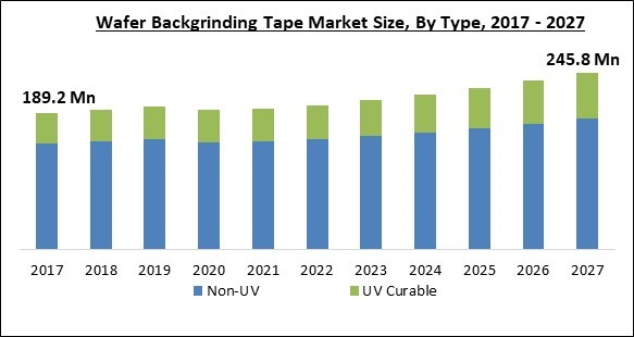
Based on type, the wafer backgrinding tape market is bifurcated into UV Curable and Non-UV. The UV curable segment acquired a significant revenue share in the wafer backgrinding tape market in 2020. UV Tape is a type of adhesive tape used in the semiconductor manufacturing process. It can be used to cover the surface of a semiconductor wafer during backgrinding and to hold the wafer in place with a ring frame during dicing. It can be used on a variety of materials, including ceramics, glass, sapphire, and so on.
Wafer Size Outlook
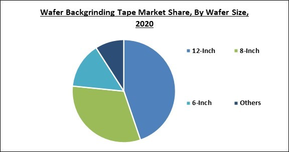
On the basis of wafer size, the wafer backgrinding tape market is segmented into 12-inch, 8-inch, 6-inch and others. The 12-inch wafer segment garnered the highest revenue share in the wafer backgrinding tape market in 2020. The larger the wafer, the more difficult it is to manufacture, and the more chips these massive wafers cut out. At the moment, 12-inch wafers are the most common in the industry, accounting for roughly 70% of total production capacity.
Regional Outlook
Region-wise, the wafer backgrinding tape market is analyzed across North America, Europe, Asia Pacific and LAMEA. Asia Pacific emerged as the leading region in the wafer backgrinding tape market with the largest revenue share in 2020. Due to a growth in demand for high voltage operational devices, organisations across verticals in this region are realising the necessity of improved semiconductor technologies to enable efficient power management. Furthermore, emerging countries such as India, the Philippines, and others are likely to provide profitable prospects for the expansion of the wafer backgrinding tape market.
The market research report covers the analysis of key stake holders of the market. Key companies profiled in the report include Furukawa Electric Co., Ltd., Mitsui Chemicals, Inc., Lintec Corporation, Nitto Denko Corporation, AI Technology, Inc., AMC Co., Ltd., Force-One Applied Materials Co., Ltd., and Denka Company Limited.
Recent Strategies Deployed in Voice User Interface Market
- Oct-2017: Mitsui Chemicals expanded its business by introducing its wholly-owned subsidiary, Mitsui Chemicals Tohcello. This subsidiary is expected to manufacture and sell the ICROSTape, a tape for semiconductor manufacturing. In addition, Mitsui Chemicals Tohcello is expected to strengthen its sales, manufacturing, and engineering services to support high-quality products along with continuing to boost and expand its film and sheet business.
- Apr-2017: LINTEC launched a tape laminator, RAD-3520F/12, and enhanced the performance of RAD-3510F/12. This tape laminator is expected to safeguard the circuit surface of the wafer at the time of the back grinding and thinning procedure of the semiconductor wafer after circuit formation.
Scope of the Study
Market Segments Covered in the Report:
By Type
- Non-UV and
- UV-Curable
By Wafer Size
- 12-Inch
- 8-Inch
- 6-Inch
- Others
By Geography
- North America
- US
- Canada
- Mexico
- Rest of North America
- Europe
- Germany
- UK
- France
- Russia
- Spain
- Italy
- Rest of Europe
- Asia Pacific
- China
- Japan
- India
- South Korea
- Singapore
- Malaysia
- Rest of Asia Pacific
- LAMEA
- Brazil
- Argentina
- UAE
- Saudi Arabia
- South Africa
- Nigeria
- Rest of LAMEA
Key Market Players
List of Companies Profiled in the Report:
- Furukawa Electric Co., Ltd.
- Mitsui Chemicals, Inc.
- Lintec Corporation
- Nitto Denko Corporation
- AI Technology, Inc.
- AMC Co., Ltd.
- Force-One Applied Materials Co., Ltd.
- Denka Company Limited
Unique Offerings from the Publisher
- Exhaustive coverage
- The highest number of market tables and figures
- Subscription-based model available
- Guaranteed best price
- Assured post sales research support with 10% customization free
Table of Contents
Companies Mentioned
- Furukawa Electric Co., Ltd.
- Mitsui Chemicals, Inc.
- Lintec Corporation
- Nitto Denko Corporation
- AI Technology, Inc.
- AMC Co., Ltd.
- Force-One Applied Materials Co., Ltd.
- Denka Company Limited


