Electron microscopy (EM) is a technique for taking high-resolution pictures of both biological and non-biological material. It is employed in biomedical research to look at the precise structure of organelles, macromolecular complexes, tissues, cells, and cells. The utilization of electrons as the source of illuminating radiation, which has extremely short wavelengths, contributes to the great resolution of EM pictures. To address particular issues, electron microscopy is combined with a range of auxiliary methods (such as thin sectioning, immuno-labeling, and negative staining.
For traditional scanning electron microscopy to work, secondary electrons must be emitted from a specimen's surface. A scanning electron microscope is the equivalent of a stereo light microscope in the EM because of its superior depth of focus. It offers intricate pictures of the surfaces of cells and entire organisms, which TEM cannot do. Additionally, it can be utilized for process control, particle size analysis, and counting. Because the image is created by rastering a focused electron beam across the specimen's surface, it is known as a scanning electron microscope.
Each point in the raster emits particles as a result of the primary electron beam's interaction with atoms close to the surface low energy secondary electrons, high-energy backscatter electrons, X-rays, and even photons. These can be gathered using a variety of detectors, and the brightness at each analogous position on a cathode ray tube can be calculated from their relative number. The final image is an enlarged image of the specimen since the size of the raster at the specimen is significantly smaller than the viewing screen of the CRT. SEMs that are properly set up (with secondary, backscatter, and X-ray detectors) can be used to examine specimen topography, atomic composition, as well as, the distribution of immuno-labels on the specimen's surface.
COVID-19 Impact Analysis
Trade and economic activity have been impacted by the COVID-19 outbreak everywhere in the world. While the small software industry for the automotive and aerospace industries is expected to suffer, the tiny software market for the healthcare and semiconductor industries is expected to grow. Production and manufacturing have been significantly impacted as a result of several countries around the world declaring statewide lockdowns and temporary closures of various industries. Trade restrictions have made the demand-supply mismatch worse. The COVID-19 pandemic will affect companies that make semiconductors for the electron microscope market in a variety of ways, both now and in the future.Market Growth Factors
Improvements In Microscopy Technology
Digitization, super-resolution, live-cell imaging, and high throughput techniques are examples of technological developments in microscopy. These advancements contribute to lower product and testing costs. A number of microscopes have developed recently, including expansion microscopes, scanning helium microscopes (SHeM), multi-view microscopes, and integrated microscopy systems. Among the most recent developments in electron microscopy and sample preparation is digital microscopy. Better sample viewing and fewer distorted images are produced by digital imaging's greater image resolution and precision. The creation of complete slide scanning equipment has accelerated the adoption of digital microscopy.Magnification And Depth Of Field Are Increased
The shortest wavelength of visible light, or about 0.4 micrometers, is the largest item that a scientist can view through a light microscope. Any object smaller than that in diameter won't reflect light and won't be seen by light-based equipment. These tiny items include individual atoms, molecules, and virus particles, to name a few. Because they do not rely on light from the visible spectrum to be reflected by them, electron microscopes may produce images of these objects. Instead, the sample being investigated is bombarded with high-energy electrons, and an image is created using information about how these electrons behaved as they were reflected and deflected by the sample.Market Restraining Factors
Lack Of Professional Expertise
Standard compound microscopes are simple for physicists and lab professionals to use, but as sophisticated microscopes are developed, trained personnel are needed. For instance, to study the characterization of chemical and biological compounds at the atomic or molecular level, atomic force scanning tunneling microscopes widely used in nanotechnology require physicists or technicians to have in-depth interdisciplinary knowledge in the area of surface physics and surface analyses. A particularly sensitive piece of technology, an electron microscope can be severely harmed by external magnetic fields and vibrations. It must be kept in working order by experienced personnel in a dedicated space.Type Outlook
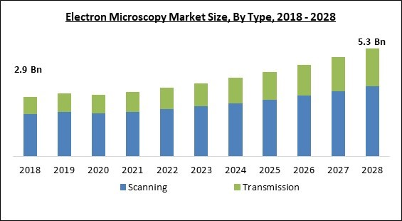
On the basis of type, the Electron Microscopy Market is divided into Scanning and Transmission. The scanning segment acquired the highest revenue share in the electron microscopy market in 2021. it is because a focused stream of high-energy electrons is utilized by scanning electron microscopes (SEMs) to produce a range of signals at the surface of solid samples. Up to 100,000x of magnification is possible with SEMs. These microscopes create 3-dimensional images with a high depth of field, high resolution (less resolution than TEMs), and information on the topography, morphology, and composition of objects.Application Outlook
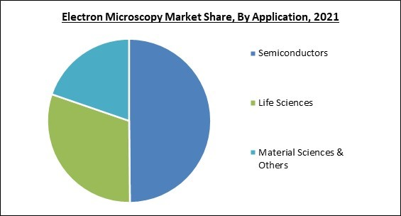
Based on the Application, the Electron Microscopy Market is classified into Semiconductors, Life Sciences, Material Sciences & Others. The life sciences segment recorded a substantial revenue share in the electron microscopy market in 2021. Biological samples are the primary focus of life science electron microscopy. This also applies to medicine development, viral testing, and testing for the food and beverage business. The subject of molecular and cellular biology in medicine has made strides because of high technology.End-User Outlook
By End-user, the Electron Microscopy Market is bifurcated into Industries, Academic & Research Institutes, and Others. The industries segment garnered the highest revenue share in the electron microscopy market in 2021. It is because pharmaceutical and biotechnology, semiconductor and electronics, textiles, mining, and material science, and natural resources (oil and gas) industries are all included in the industries segment's preview. When developing and producing semiconductors and other types of electronics, the electronics industry uses electron microscopes for high-resolution imaging.Regional Outlook
Region-wise, the Electron Microscopy Market is analyzed across North America, Europe, Asia Pacific, and LAMEA. The Asia pacific region acquired a promising revenue share in the electron microscopy market in 2021. The Asia Pacific is fueled due to the factors such as the rising R&D funding for microscopy research, expanding use of correlative microscopy in life science and nanotechnology research, the establishment of collaboration centers for microscopy research, and the affordability of raw materials and skilled labor for OEMs.Cardinal Matrix - Electron Microscopy Market Competition Analysis
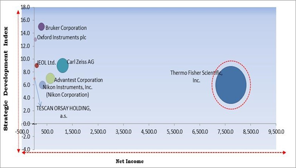
The major strategies followed by the market participants are Product Launches. Based on the Analysis presented in the Cardinal matrix; Thermo Fisher Scientific, Inc. is the forerunners in the Electron Microscopy Market. Companies such as Advantest Corporation, Carl Zeiss AG, Bruker Corporation are some of the key innovators in Electron Microscopy Market.
The market research report covers the analysis of key stake holders of the market. Key companies profiled in the report include Bruker Corporation, Carl Zeiss AG, Thermo Fisher Scientific, Inc., JEOL Ltd., Nikon Instruments, Inc. (Nikon Corporation), Hitachi High-Technologies Corporation (Hitachi Ltd.), Oxford Instruments plc, TESCAN ORSAY HOLDING, a.s., Delong Instruments AS, and Advantest Corporation.
Strategies deployed in Electron Microscopy Market
» Partnerships, Collaborations and Agreements:
- Jun-2022: ZEISS Microscopy came into a partnership with LabCentral, a non-profit organization founded as a launchpad for biotech start-ups. Together, the companies aimed to deliver image analysis and innovative microscopy resources to high-potential life science investigators in a two-year incubator program.
- May-2022: Bruker Corporation came into a partnership with TOFWERK, A Global Leader in TOF Mass Spectrometry. With this partnership, the companies aimed to deliver ultra-sensitive, high-speed spread and industrial analytical solutions, in convergence with a Bruker minority investment in TOFWERK. Moreover, the companies offer a basis for technology collaborations to promote instrument abilities and for the growth of novel analytical applications where ultra-sensitivity and high-speed matter.
» Product Launches and Product Expansions:
- Jun-2022: Bruker Corporation launched XFlash 7 detector series for its QUANTAXTM energy dispersive X-ray spectrometer systems. The new XFlash 7 detector series allow a chemical breakdown of material models in electron microscopes with maximum sensitivity, speed, and dependability.
- Apr-2022: Advantest Corporation launched the Euclid, a new 3D image observer for its Hadatomo series of photoacoustic microscopes. The new Euclid can portray 3D images by superimposing data on the melanin in the vascular network, the skin, and the skin structure, as estimated by a Hadatomo tool, and can also efficiently form tomographic pictures. Additionally, picture production requirements can be imported as a composition file, allowing easy differentiation of measurement data.
- Mar-2022: Imaris, an Oxford Instruments company introduced Imaris 9.9, the modern version of microscopy image analysis software. The new Imaris 9.9 is the most brilliant and adaptable version ever, offering segmentation with machine learning, along with open-source connections. Moreover, the addition of machine learning pixel classification, with a reflexive and interactive training mode, widens the variety of images for research as it allows electron microscopy segmentation and shapes identification.
- Jan-2022: JEOL USA Inc, a wholly-owned subsidiary of JEOL unveiled JSM-IT510, a new scanning electron microscope providing automated montaging, automated imaging, and live EDS analysis. The new IT510 features JEOL Intelligent Technology allows easy navigation from optical to SEM imaging, Live EDS and 3D analysis, and auto operations from alignment to focus for clear, fast, and sharp pictures.
- Dec-2021: Nikon Instruments launched the Digital Sight 10 Microscope Camera. The new camera allows the addition of both monochrome and color photos with a resolution of 6K pixels within a large field of view utilizing a single camera.
- Nov-2021: Nikon Instruments unveiled AX R MP multiphoton confocal microscope. The new device provides a large area of view images, high resolution, within living organisms at a quick speed.
- Nov-2021: JEOL launched the JSM-IT510 series, a new scanning electron microscope. The new JSM-IT510 series is launched to fulfill the requirements and increase throughput, developed JSM-IT510 series, which also develops the operability of JEOL famous InTouchScope. Additionally, SEM applications are expanding for basic research along with quality control at manufacturing locations.
- Sep-2021: Imaris, an Oxford Instruments label launched Imaris 9.8, the advanced version of its market-leading microscopy image analysis software. The new Imaris 9.8 provides entity visualization on raised sections, jointly with the raw information which unlocks new ways of validating discovery and cleansing in Imaris. Additionally, consumers can see the accuracy of the Spots and Surfaces detection, even in a “messy” data volume with thousands of things.
- Jul-2021: Thermo Fisher Scientific introduced Thermo Scientific Phenom Pharos G2 Desktop Field Emission Gun, Scanning Electron Microscope. The new FEG-SEM is designed to extend the permit to advanced nanomaterial research abilities. Additionally, The new device makes it possible for consumers to utilize a tabletop microscope to intuitively characterize the shape, size, and chemical design of a broad range of nanoparticles at high resolution.
- Jul-2021-Jul Tescan Orsay introduced the AutoSlicer module for the semi-automated transmission electron microscope. the new TESCAN’s AutoSlicer allows high output TEM specimen practice at numerous sites or on various samples and delivers full authority over the specific parameters required for optimal sample quality for both Plasma FIB-SEM instruments and Gallium (Ga) focused ion beam (FIB)-scanning electron microscope (SEM).
- Jun-2021: Hitachi High-Tech introduced AFM100 along with AFM100 Plus systems, entry-level and advanced-level models of Hitachi’s concise and adaptable Atomic Force Microscopes. The new devices are developed to deliver comfort of use and prominent dependability for high-throughput R&D or grade control applications.
- Feb-2021: Thermo Fisher Scientific launched Helios 5 PXL Wafer DualBeam, a plasma-focused ion beam scanning electron microscope. The new Helios 5 PXL can decrease time-to-data from days to hours for inline via-stack metrology and verify high-aspect-ratio systems. Additionally, The microscope has high-contrast imaging, high-resolution, and large-area sample preparation, oblique milling, and cross-sectioning of 3D semiconductor instruments.
- Nov-2020: ZEISS introduced ZEISS GeminiSEM, a new generation of its field emission scanning electron microscope. The ZEISS GeminiSEM new models 360, 460, and 560 are designed for sub-nanometer imaging and intuitive analytics. Additionally, The new ZEISS GeminiSEM family produces more information from any model, decreases sample damage, and retains sample artifacts.
- Oct-2020: The Bruker Nanomechanical Testing business unveiled Hysitron PI 89 SEM PicoIndenter. The new system delivers nanomechanical testing abilities within a scanning electron microscope (SEM) at higher loads and in more severe conditions than earlier possible. Additionally, the Hysitron PI 89 SEM PicoIndenter integrates Bruker’s high-performance regulator with unique resistive transducer and intrinsic removal technologies to allow unmatched power and displacement ranges.
- Jul-2020: JEOL unveiled the JSM-IT800 FE-SEM, the most powerful Scanning electron microscope. The new microscope delivers two models with two types of objective lenses such as the Hybrid Lens for general-purpose SEM and the Super Hybrid Lens for improved resolution obedience and diverse analyses. Additionally, the JSM-IT800 FE-SEM delivers a resolution of 0.5nm @ 15kV and 0.9nm at 500V.
- Jun-2020: Bruker launched Flash XS, a new electron backscatter diffraction (EBSD) detector. The new e-Flash XS allows the analysis of the microstructure of crystalline materials in tabletop and other small, entry-level scanning electron microscopes (SEM).
- Jun-2020: Oxford Instruments NanoAnalysis unveiled Relate, an image analysis software platform. The new software supplies a highly precise interaction of EDS, EM, EBSD, and AFM data for the consumer of Oxford Instrument’s superior-edge materials description tools, in association with Digital Surf, founder of the industry-standard Mountains surface and image analysis software forum.
» Acquisitions and Mergers:
- Jun-2022: Advantest Corporation took over Collaudi Elettronici Automatizzati, an Italy-based enterprise. With this acquisition, CREA is expected to expand Advantest Corporation's trial and measurement solutions within the evolving semiconductor value chain to fulfill a broader capacity of consumer demands.
- Nov-2021: Bruker Corporation took over MOLECUBES, a vibrant developer in benchtop preclinical nuclear molecular imaging (NMI) systems. With this acquisition, Bruker reinforces its position as a foremost NMI solutions supplier in translational and preclinical imaging research.
- Jun-2021: Oxford Instruments completed the acquisition of WITec Wissenschaftliche Instrumente und Technologie GmbH, a leading supplier of Raman microscopy imaging solutions. With this acquisition, the company aimed to sustain consumers in stunning end markets, improving its offering of solutions for a variety of applications such as life science, semiconductors, and advanced materials.
- Dec-2020: Zeiss completed the acquisition of the Arivis, a scientific imaging platform. With this acquisition, Zeiss aimed to reinforce its software capabilities and market position in image processing, 3D image visualization, and examination software for research microscopy.
Scope of the Study
Market Segments Covered in the Report:
By Type
- Scanning
- Transmission
By Application
- Semiconductors
- Life Sciences
- Material Sciences & Others
By End User
- Industries
- Academic & Research Institutes
- Others
By Geography
- North America
- US
- Canada
- Mexico
- Rest of North America
- Europe
- Germany
- UK
- France
- Russia
- Spain
- Italy
- Rest of Europe
- Asia Pacific
- China
- Japan
- India
- South Korea
- Singapore
- Malaysia
- Rest of Asia Pacific
- LAMEA
- Brazil
- Argentina
- UAE
- Saudi Arabia
- South Africa
- Nigeria
- Rest of LAMEA
Key Market Players
List of Companies Profiled in the Report:
- Bruker Corporation
- Carl Zeiss AG
- Thermo Fisher Scientific, Inc.
- JEOL Ltd.
- Nikon Instruments, Inc. (Nikon Corporation)
- Hitachi High-Technologies Corporation (Hitachi Ltd.)
- Oxford Instruments plc
- TESCAN ORSAY HOLDING, a.s.
- Delong Instruments AS
- Advantest Corporation
Unique Offerings from the Publisher
- Exhaustive coverage
- The highest number of Market tables and figures
- Subscription-based model available
- Guaranteed best price
- Assured post sales research support with 10% customization free
Table of Contents
Companies Mentioned
- Bruker Corporation
- Carl Zeiss AG
- Thermo Fisher Scientific, Inc.
- JEOL Ltd.
- Nikon Instruments, Inc. (Nikon Corporation)
- Hitachi High-Technologies Corporation (Hitachi Ltd.)
- Oxford Instruments plc
- TESCAN ORSAY HOLDING, a.s.
- Delong Instruments AS
- Advantest Corporation


