Extreme ultraviolet lithography, or EUVL, is one of the leading next-generation lithography (NGL) techniques used to print lines as thin as 30 nm and create microprocessors and microchips. This novel and advanced technology are significantly being employed to design microcircuits. Strong ultraviolet laser beams that are reflected off of a silicon wafer are burned into the silicon wafer by the EUVL technology. A further extremely short wavelength solution that can be used up to the 10nm node is extreme UV lithography systems.
Extreme ultraviolet lithography is an optical lithography process that creates patterns by exposing reflective photomask to UV light, which is reflected onto a substrate covered in the photoresist. This process uses a range of extreme ultraviolet wavelengths, approximately encompassing a 2% FWHM bandwidth of about 13.5 nm. It is frequently used in the process of creating semiconductor devices.
Because EUVL systems are more advanced technologically than other lithography methods, the market for them is anticipated to develop significantly throughout the coming years. Additionally, the market for extreme-ultraviolet lithography technologies is anticipated to rise due to the imminent need for smaller electronic devices. Additionally, an increase in microelectronics device sales is anticipated to fuel the market for extreme-ultraviolet lithography equipment in the coming years.
By reflecting light, several alternating layers of silicon and molybdenum are used to create EUV photomasks. In contrast, traditional photomasks block the light using a single layer of chromium on a quartz substrate. A EUV mask is made up of 40 layers of silicon and molybdenum that alternate, acting as a multilayer to reflect the extreme ultraviolet light via Bragg diffraction. The wavelength and incident angle have a significant impact on the reflectance, with shorter wavelengths reflecting away from normal incidence and longer wavelengths reflecting near-normal incidence.
COVID-19 Impact Analysis
Due to a major impact on key companies in the supply chain, the COVID-19 outbreak had a significant impact on the growth of the extreme ultraviolet lithography systems market. In addition, the COVID-19 pandemic caused a number of challenges for the market, including a shortage of competent workers and delays or cancellations of projects due to full or partial lockdown, globally. Moreover, the transmission of coronavirus was rapid, and the semiconductor industry was been shut down entirely due to the lockdown imposed by governments of various countries. Because industrial automation tools boost corporate efficiency and cut labor expenses, many businesses use them in their operations.Market Growth Factors
Rising Utilization Of Smartphones
The technological infrastructure, information and communication technologies available to the service to be offered, the access of the end-users to the service, and the service's usability are only a few of the factors that need to be considered while developing smart services. Additionally, there are other reasons that are readily available, such as the quick expansion of smart devices, the excellence of mobile networks, and the rising need for highly effective smart applications. The essential principles in the framework for smart government must be used when providing information services via mobile phones and smart platforms.Increasing Growth Of The Pharmaceuticals Industry
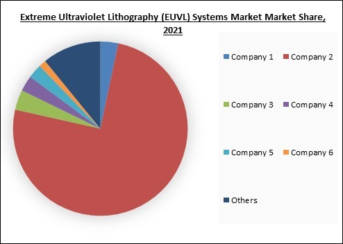
With the introduction of new technology as well as more economical and effective manufacturing techniques, the pharmaceutical industry has experienced a significant transition. Additionally, the market growth has been positively driven by rising investment flow in this sector. The use of robotics and artificial intelligence reduces downtime on the manufacturing floor and the production of product waste (AI). Additionally, single-use disposable products have been launched in this market, replacing traditional open transfer manufacturing methods. Additionally, the paradigm change towards integrated, intelligent, and data-rich paperless operations has produced accurate and error-free output. Such continuous discoveries have accelerated the production of drugs.The leading players in the market are competing with diverse innovative offerings to remain competitive in the market. The below illustration shows the percentage of revenue shared by some of the leading companies in the market. The leading players of the market are adopting various strategies in order to cater demand coming from the different industries. The key developmental strategies in the market are Acquisitions, and Partnerships & Collaborations.
Marketing Restraining Factor:
Prevalence Of Alternatives Across The Market
An image is projected into a photosensitive emulsion that has been put on a substrate, such as a silicon wafer, in the process of optical lithography, a photon-based process. The semiconductor industry uses this optical lithography technique the most for producing Nano-electronics in large quantities. The widespread usage of optical lithography is directly related to the technology's extremely parallel architecture, which enables the quick transport of enormous volumes of data. For instance, cutting-edge lithography equipment today can print 150-300 mm wafers per hour with a 40-nm two-dimensional pattern resolution, which results in a throughput of about 1.8T pixels/s.Equipment Outlook
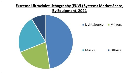
By the Equipment, the Extreme Ultraviolet Lithography Systems Market is segregated into Mask, Light Source, Mirrors, and Others. In 2021, the mirrors segment witnessed a substantial revenue share of the extreme ultraviolet lithography systems market. For extreme ultraviolet lithography, there are no lenses. The lenses is expected to absorb the light in the system because most materials absorb EUV light. In modern systems, manufacturers are integrating a new optical system that utilizes multilayer mirrors that are ultra-smooth in a vacuum chamber.Regional Outlook
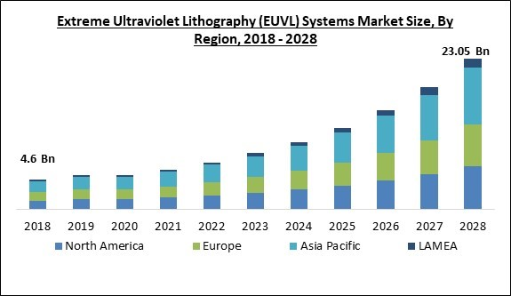
Region-Wise, the Extreme Ultraviolet Lithography Systems Market is analyzed across North America, Europe, Asia-Pacific, and LAMEA. In 2021, Asia Pacific accounted for the highest revenue share of the extreme ultraviolet lithography market. The surging growth of the regional market is attributed to the constantly expanding semiconductor industry of the region. China in particular continues to be a prominent player in the market for extreme-ultraviolet lithography systems in Asia-Pacific. Major businesses and government agencies in the nation are heavily investing in technology, which is also a major factor driving the growth of the segment.The market research report covers the analysis of key stake holders of the market. Key companies profiled in the report include Intel Corporation, Samsung Electronics Co., Ltd. (Samsung Group), Toshiba Corporation, Carl Zeiss AG, Nikon Corporation, ASML Holding N.V., Canon, Inc., Taiwan Semiconductor Manufacturing Company Limited, Toppan Inc., and NTT Advanced Technology Corporation (Nippon Telegraph and Telephone Corporation).
Scope of the Study
Market Segments Covered in the Report:
By Equipment
- Light Source
- Laser Produced Plasmas (LPP)
- Vacuum Sparks
- Gas Discharges
- Mirrors
- Masks
- Others
By Geography
- North America
- US
- Canada
- Mexico
- Rest of North America
- Europe
- Germany
- UK
- France
- Russia
- Spain
- Italy
- Rest of Europe
- Asia Pacific
- China
- Japan
- India
- South Korea
- Singapore
- Malaysia
- Rest of Asia Pacific
- LAMEA
- Brazil
- Argentina
- UAE
- Saudi Arabia
- South Africa
- Nigeria
- Rest of LAMEA
Key Market Players
List of Companies Profiled in the Report:
- Intel Corporation
- Samsung Electronics Co., Ltd. (Samsung Group)
- Toshiba Corporation
- Carl Zeiss AG
- Nikon Corporation
- ASML Holding N.V.
- Canon, Inc.
- Taiwan Semiconductor Manufacturing Company Limited
- Toppan Inc.
- NTT Advanced Technology Corporation (Nippon Telegraph and Telephone Corporation)
Unique Offerings from the Publisher
- Exhaustive coverage
- The highest number of market tables and figures
- Subscription-based model available
- Guaranteed best price
- Assured post sales research support with 10% customization free
Table of Contents
Companies Mentioned
- Intel Corporation
- Samsung Electronics Co., Ltd. (Samsung Group)
- Toshiba Corporation
- Carl Zeiss AG
- Nikon Corporation
- ASML Holding N.V.
- Canon, Inc.
- Taiwan Semiconductor Manufacturing Company Limited
- Toppan Inc.
- NTT Advanced Technology Corporation (Nippon Telegraph and Telephone Corporation)


