Free Webex Call
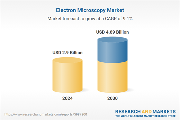
Global Electron Microscopy Market was valued at USD 2.14 Billion in 2023 and is anticipated to project impressive growth in the forecast period with a CAGR of 8.47% through 2029. The Global Electron Microscopy Market is primarily driven by advancements in technology, which have led to the development of high-resolution electron microscopes capable of capturing detailed images at the nanoscale level. These technological innovations have significantly expanded the applications of electron microscopy across various fields such as materials science, life sciences, and semiconductor industries. The increasing demand for nanotechnology research and the study of complex biological structures are driving the adoption of electron microscopy techniques. The growing prevalence of chronic diseases and infectious diseases has created a need for advanced diagnostic tools, wherein electron microscopy plays a crucial role in understanding disease mechanisms and developing therapeutic interventions. Government initiatives aimed at funding research projects and academic institutions' focus on enhancing scientific research capabilities are contributing to the market growth of electron microscopy worldwide.Speak directly to the analyst to clarify any post sales queries you may have.
10% Free customizationThis report comes with 10% free customization, enabling you to add data that meets your specific business needs.
Key Market Drivers
Technological Advancements
The Global Electron Microscopy Market experiences relentless momentum, primarily propelled by the perpetual evolution of technology within electron microscopy systems. These advancements herald a new era of microscopy, characterized by unparalleled precision and resolution. Innovations such as aberration-corrected electron optics, revolutionary electron sources, and cutting-edge detectors have collectively ushered in a paradigm shift in imaging capabilities. With these advancements, electron microscopes have transcended previous limitations, enabling researchers to delve into the intricate world of nanoscale structures with unprecedented clarity and precision.Aberration-corrected electron optics represent a breakthrough in electron microscopy, mitigating distortions and aberrations that traditionally hindered imaging accuracy. This correction mechanism ensures that images captured by electron microscopes faithfully represent the actual structure of specimens, providing researchers with unparalleled insights into their composition and morphology. These technological advancements collectively empower researchers to explore complex structures with unprecedented clarity and resolution, unraveling mysteries at the nanoscale level that were once beyond the realm of visualization. In April 2024, researchers in Manchester are pioneering the development of a revolutionary Transmission Electron Microscope (TEM), the first of its kind globally, which seamlessly integrates state-of-the-art imaging and spectroscopy with artificial intelligence and automated workflows, known as AutomaTEM. As electron microscopy continues to evolve, driven by innovation and scientific curiosity, its transformative impact on research and discovery across diverse fields is poised to accelerate, opening new frontiers in science, technology, and beyond.
Increasing Demand from Life Sciences
The life sciences sector stands at the forefront of driving growth within the electron microscopy market, exerting profound influence due to the indispensable role electron microscopy techniques play in advancing biological research. Widely utilized across various disciplines within life sciences, electron microscopy serves as a cornerstone for investigating intricate cellular structures, subcellular organelles, viruses, proteins, and diverse biological molecules. The escalating demand for cutting-edge imaging methodologies, particularly in fields like structural biology, cell biology, neuroscience, and microbiology, underscores the pivotal significance of electron microscopy. Researchers rely on electron microscopy's unparalleled ability to capture high-resolution images at the nanoscale level, enabling them to unravel the complexities of fundamental life processes with unprecedented detail and precision. As scientific exploration delves deeper into understanding the intricacies of living organisms, electron microscopy emerges as an indispensable tool, driving innovation and discovery within the realm of life sciences.Rising Demand from Material Sciences
Electron microscopy stands as an indispensable tool in the realm of material sciences research and development, offering unparalleled insights into the intricate world of materials at the atomic and molecular scale. This capability enables researchers to delve deep into the microstructure, morphology, composition, and properties of diverse materials with exceptional precision, revolutionizing our understanding of their behavior and functionality.Two primary techniques, scanning electron microscopy (SEM) and transmission electron microscopy (TEM), serve as the cornerstone of electron microscopy applications in material sciences. SEM allows for the detailed imaging of surface structures, offering high-resolution, three-dimensional views that unveil the topography and morphology of materials. On the other hand, TEM delves even deeper, providing cross-sectional imaging and atomic-scale resolution, enabling the visualization of internal structures and atomic arrangements within materials. The widespread adoption of electron microscopy techniques has permeated across various industries, including semiconductor, automotive, aerospace, electronics, and nanotechnology. In the semiconductor industry, electron microscopy plays a pivotal role in material characterization, process optimization, and quality control. SEM and TEM are instrumental in analyzing semiconductor devices, examining thin films, and investigating defects, contributing to the advancement of semiconductor technology and the development of cutting-edge electronic devices. For instance, in the last ten years, cryo-electron microscopy (cryoEM) has emerged as a potent technique for elucidating intricate structures of complex molecules. Presently, a novel design developed by scientists at the Medical Research Council’s Laboratory of Molecular Biology (MRC-LMB) in the United Kingdom, along with their partners which holds the potential to reduce the cost of cryoEM by as much as 90 percent. This breakthrough could democratize structural studies in biology and material science, making them accessible to researchers who currently rely on regional centers or colleagues from more financially endowed institutions to analyze their samples.
Growing Adoption in Nanotechnology
The increasing adoption of nanotechnology in various industries is driving the demand for electron microscopy. Nanotechnology involves the manipulation and engineering of materials at the nanoscale level to create novel structures and devices with unique properties and functionalities. Electron microscopy is indispensable for visualizing and characterizing nanomaterials, nanostructures, and nanodevices, facilitating research and development in areas such as nanoelectronics, nanomedicine, nanomaterials, and nanocomposites.Key Market Challenges
Technological Complexity and Cost
One of the significant challenges facing the global electron microscopy market is the complexity and cost associated with advanced electron microscopy systems. While these systems offer unparalleled resolution and imaging capabilities, they often require specialized training and expertise to operate effectively. The high initial investment and ongoing maintenance costs pose a barrier to adoption for many research institutions and laboratories, particularly those with limited financial resources. Addressing these challenges requires innovative approaches to reduce the complexity and cost of electron microscopy systems while maintaining their performance and reliability.Sample Preparation and Handling
Another challenge in electron microscopy is the sample preparation and handling process, which can be time-consuming, labor-intensive, and prone to artifacts. Achieving high-quality imaging results often requires meticulous sample preparation techniques, including fixation, dehydration, embedding, sectioning, and staining. The delicate nature of many samples, such as biological specimens or nanomaterials, necessitates careful handling to avoid damage or contamination during preparation and imaging. Streamlining sample preparation workflows and developing automated sample handling systems are critical areas for improvement to enhance the efficiency and reproducibility of electron microscopy experiments.Key Market Trends
Expanding Applications in Semiconductor Industry
The semiconductor industry is a key end-user of electron microscopy for process development, quality control, and failure analysis. Electron microscopy techniques such as SEM and TEM are widely used in the semiconductor industry for inspecting semiconductor devices, analyzing semiconductor materials, and characterizing nanostructures and thin films. With the continuous miniaturization of semiconductor devices and the development of advanced materials and fabrication techniques, the demand for electron microscopy in the semiconductor industry is expected to grow significantly.Government Initiatives and Funding
Government initiatives and funding support for scientific research and development are driving the growth of the electron microscopy market. Governments around the world are investing in research infrastructure, academic institutions, and research organizations to promote scientific innovation and technological advancement. Funding programs, grants, and collaborations are fostering research projects that leverage electron microscopy techniques to address key scientific challenges and societal needs, thereby fueling the demand for electron microscopy systems and services.Segmental Insights
Type Insights
Based on the type, the Transmission Electron Microscope (TEM) stands out as the dominant technology, revolutionizing the way researchers visualize and analyze samples at the nanoscale level. TEM offers unparalleled resolution and imaging capabilities, making it indispensable in a wide range of scientific disciplines, including materials science, biology, nanotechnology, and semiconductor research.One of the key factors driving the dominance of TEM in the electron microscopy market is its exceptional resolution capabilities. TEM can achieve sub-nanometer resolution, allowing researchers to observe individual atoms and molecules with unprecedented detail. This high resolution enables the study of nanomaterials, nanoparticles, biological structures, and semiconductor devices at the atomic level, providing valuable insights into their structure, morphology, composition, and properties. TEM offers versatile imaging modes and techniques, making it suitable for a diverse range of applications. From conventional bright-field imaging to advanced techniques such as high-resolution TEM (HRTEM), electron diffraction, and energy-dispersive X-ray spectroscopy (EDS), TEM provides researchers with a comprehensive toolkit for characterizing materials and analyzing their properties. This versatility makes TEM indispensable in research fields such as materials science, where understanding the structure-property relationships of materials is critical for developing advanced materials with tailored properties.
End User Insights
Based on the end user, Academic & Research Institutions emerge as the dominant users, driving the demand for electron microscopy systems and services. These institutions play a pivotal role in advancing scientific research across diverse fields, including materials science, biology, nanotechnology, and semiconductor technology. One of the key reasons for the dominance of Academic & Research Institutions in the electron microscopy market is their diverse range of research activities and applications. Academic institutions are at the forefront of scientific exploration, conducting fundamental research to unravel the mysteries of nature and develop innovative technologies. Electron microscopy serves as a cornerstone tool for researchers in these institutions, enabling them to visualize and analyze materials at the nanoscale level with unparalleled detail and precision.Academic & Research Institutions often have dedicated facilities and laboratories equipped with state-of-the-art electron microscopy systems. These facilities cater to a wide range of research needs, providing access to advanced microscopy techniques and instrumentation for faculty, students, and collaborators. The availability of such infrastructure fosters a collaborative research environment and facilitates interdisciplinary studies across various scientific disciplines. Academic & Research Institutions drive demand for electron microscopy through their contributions to scientific publications, conferences, and collaborative projects. Researchers from these institutions regularly publish groundbreaking research papers that showcase the capabilities of electron microscopy in elucidating fundamental scientific phenomena and solving real-world problems. These publications not only highlight the importance of electron microscopy in academic research but also drive awareness and interest among industry stakeholders and policymakers.
Regional Insights
North America emerges as the dominant region, wielding substantial influence and driving significant demand for electron microscopy systems and services. Several key factors contribute to North America's dominance in this market, solidifying its position as a frontrunner in the field of advanced microscopy technologies. One of the primary drivers behind North America's leadership in the Electron Microscopy Market is the region's robust research and development (R&D) ecosystem. North America is home to numerous world-renowned academic institutions, research organizations, and technology companies that actively engage in cutting-edge scientific exploration and innovation. These entities leverage electron microscopy as a vital tool for investigating materials, biological specimens, and nanoscale structures, driving the demand for sophisticated microscopy solutions.The presence of leading manufacturers and suppliers of electron microscopy equipment and services further bolsters North America's dominance in the market. The region hosts several prominent companies specializing in the development, production, and distribution of electron microscopes, accessories, and related software solutions. These industry players capitalize on the region's advanced technological infrastructure, skilled workforce, and extensive network of research collaborators to deliver state-of-the-art electron microscopy systems tailored to diverse scientific applications.
Key Market Players
- Merck KGaA
- JEOL Ltd.
- Carl Zeiss AG
- Danaher Corporation
- Olympus Corporation
- Nikon Instruments, Inc.
- Hitachi High-Technologies Corporation
- Oxford Instruments plc
- Bruker Corporation
- Hirox Europe
Report Scope:
In this report, the Global Electron Microscopy Market has been segmented into the following categories, in addition to the industry trends which have also been detailed below:Electron Microscopy Market, By Type:
- Scanning Electron Microscope
- Transmission Electron Microscope
- Reflection Electron Microscope
- Field Emission Scanning Electron Microscope
Electron Microscopy Market, By Product Type:
- Tabletop/Benchtop
- Conventional
Electron Microscopy Market, By Application:
- Lifesciences
- Earth & Environmental Sciences
- Material Sciences
- Semi-conductors
- Others
Electron Microscopy Market, By End User:
- Hospitals & Clinics
- Industries
- Academic & Research Institutions
- Others
Electron Microscopy Market, By Region:
- North America
- United States
- Canada
- Mexico
- Europe
- France
- United Kingdom
- Italy
- Germany
- Spain
- Asia-Pacific
- China
- India
- Japan
- Australia
- South Korea
- South America
- Brazil
- Argentina
- Colombia
- Middle East & Africa
- South Africa
- Saudi Arabia
- UAE
Competitive Landscape
Company Profiles: Detailed analysis of the major companies present in the Global Electron Microscopy Market.Available Customizations:
Global Electron Microscopy market report with the given market data, the publisher offers customizations according to a company's specific needs. The following customization options are available for the report:Company Information
- Detailed analysis and profiling of additional market players (up to five).
This product will be delivered within 1-3 business days.
Table of Contents
1. Product Overview
2. Research Methodology
3. Executive Summary
5. Global Electron Microscopy Market Outlook
6. North America Electron Microscopy Market Outlook
7. Europe Electron Microscopy Market Outlook
8. Asia-Pacific Electron Microscopy Market Outlook
9. South America Electron Microscopy Market Outlook
10. Middle East and Africa Electron Microscopy Market Outlook
11. Market Dynamics
12. Market Trends & Developments
13. Porter’s Five Forces Analysis
14. Competitive Landscape
Companies Mentioned (Partial List)
A selection of companies mentioned in this report includes, but is not limited to:
- Merck KGaA
- JEOL Ltd.
- Carl Zeiss AG
- Danaher Corporation
- Olympus Corporation
- Nikon Instruments, Inc.
- Hitachi High-Technologies Corporation
- Oxford Instruments plc
- Bruker Corporation
- Hirox Europe