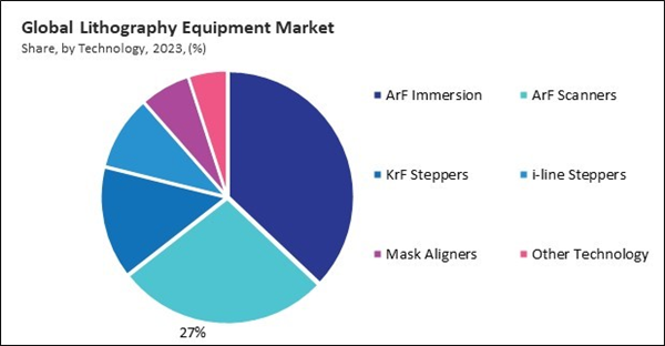
KrF steppers are driven by the demand for moderate-resolution patterning at a 248 nm wavelength, suitable for applications that do not require the ultra-fine features achievable with ArF immersion or scanners. Hence, the KrF steppers segment procured 14% revenue share in the market in 2023. KrF lithography is often employed in fabricating power electronics and certain integrated circuits, especially those used in automotive and industrial applications. The expanding demand for IoT devices, power management, and automotive electronics supports the continued use of KrF steppers, which provide the necessary balance between performance and cost efficiency.
5G technology is rapidly advancing globally, requiring semiconductors that support high-speed, low-latency data transmission. Chips manufactured using EUV and DUV lithography meet the power density and performance standards required for 5G and its related applications, such as IoT and autonomous systems. Consequently, semiconductor manufacturers are investing heavily in EUV and DUV lithography equipment to address these growing demands, driving the market growth. Additionally, the Internet of Things (IoT) revolution has inaugurated a new era of connectivity.
Semiconductors are essential for the real-time processing and transmission of data in a variety of devices, including industrial sensors, smart home appliances, and healthcare monitoring systems. This trend, in turn, has increased the reliance on sophisticated lithography equipment that can meet these high-performance standards. Hence, these factors are driving market growth.
However, For SMEs, the financial strain of purchasing such high-cost equipment can limit their ability to compete effectively, creating an entry barrier that slows market growth and restricts innovation among smaller players. Even after the initial investment, maintenance costs are also high, as EUV machines require regular servicing by highly trained professionals and ongoing technical support to ensure optimal performance. Hence, the combined cost of acquisition and maintenance creates a heavy financial burden, pushing many potential market participants out of the running and slowing down the lithography equipment market’s growth.
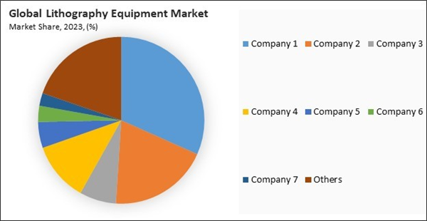
The leading players in the market are competing with diverse innovative offerings to remain competitive in the market. The above illustration shows the percentage of revenue shared by some of the leading companies in the market. The leading players of the market are adopting various strategies in order to cater demand coming from the different industries. The key developmental strategies in the market are Acquisitions, and Partnerships & Collaborations.
Driving and Restraining Factors
Drivers
- Rising Demand for Semiconductors
- Rapid Advancements in Technology
- Growing Adoption of Artificial Intelligence (AI) and the Internet of Things (IoT)
Restraints
- High Cost of Equipment and Maintenance
- Long R&D and Production Cycles
Opportunities
- Government and Corporate Investments
- Increasing Complexity of Chip Designs
Challenges
- Competition From Alternative Technologies
- Limited Access to Raw Materials
Type Outlook
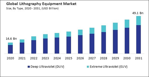
Based on type, the market is bifurcated into deep ultraviolet (DUV) and extreme ultraviolet (EUV). The extreme ultraviolet (EUV) segment procured 22% revenue share in the market in 2023. EUV lithography enables the production of circuits with finer resolutions, supporting innovations in fields like artificial intelligence, 5G, and high-performance computing, where miniaturization and processing power are critical. Although EUV systems are costlier and more technically complex than DUV, their ability to support cutting-edge technology and meet stringent performance requirements fuels their adoption.Application Outlook
On the basis of application, the market is classified into advanced packaging, LED, MEMS, and power devices. The advanced packaging segment acquired 39% revenue share in the market in 2023. The growing demand for high-performance, miniaturized electronic devices is the reason for this dominance, as they necessitate sophisticated packaging solutions to improve their efficacy and efficiency. In order to meet the required interconnect densities and performance metrics, advanced packaging techniques, including system-in-package (SiP) and 3D integration, heavily depend on precise lithography processes.Technology Outlook
By technology, the market is divided into ArF immersion, ArF scanners, KrF steppers, i-line steppers, mask aligners, and others. The ArF scanners segment garnered 27% revenue share in the market in 2023. ArF scanners are propelled by the semiconductor industry's demand to produce fine patterns without the complexities of immersion. Operating at a 193 nm wavelength, ArF scanners allow for accurate patterning, suitable for high-density applications where moderate precision suffices. This technology is widely used to produce memory and logic chips, essential for consumer electronics and data center applications.Packaging Platforms Outlook
Based on packaging platforms, the market is segmented into 3D IC, 2.5D Interposer, wafer level chip scale packaging (WLCSP), FO WLP wafer, 3D WLP, and others. The 3D IC segment acquired 36% revenue share in the market in 2023. This success is attributable to the increasing demand for miniaturized, high-performance electronic devices, which require sophisticated packaging solutions to enhance their efficiency and effectiveness. 3D ICs stack multiple semiconductors dies vertically and offer significant performance and space utilization advantages, making them essential in applications such as smartphones, data centers, and high-performance computing.Regional Outlook
Region-wise, the market is analyzed across North America, Europe, Asia Pacific, and LAMEA. The Asia Pacific segment garnered 42% revenue share in the market in 2023. The Asia Pacific region, comprising major semiconductor-producing countries like Taiwan, South Korea, Japan, and China, captured the largest revenue share in the lithography equipment market in 2023. This dominance is driven by industry giants such as TSMC, Samsung, and SMIC, who are at the forefront of semiconductor manufacturing. In China and South Korea, the demand for sophisticated lithography equipment has significantly increased as a result of government support and investment in local semiconductor industries.Recent Strategies Deployed in the Market
- Oct-2024: Canon has delivered its first nanoprint lithography machine, the FPA-1200NZ2C, to the Texas Institute for Electronics. This cost-effective alternative to ASML's technology can produce semiconductors down to 5nm nodes and aims to support smaller manufacturers in the industry.
- Jun-2024: Canon has launched its nanoimprint lithography technology in India, enabling chip designs to be stamped onto silicon wafers. This new equipment consumes less power and will support India's semiconductor industry by providing skill development training for engineers and expanding into the medical sector.
- Feb-2024: Nikon Corporation is broadening its lithography business by expanding its customer base beyond Intel to include markets in South Korea, China, and Southeast Asia. The company provides a range of semiconductor lithography equipment, including i-line and ArF immersion machines.
- Feb-2024: Applied Materials has expanded its patterning solutions portfolio for angstrom-era chipmaking, introducing new etch systems, CVD films, and metrology tools. The Sculpta® pattern-shaping technology aims to enhance yield and reduce costs for 2nm and below process nodes.
- Nov-2023: EV Group and Silicon Austria Labs have expanded their collaboration by installing advanced lithography systems, including the LITHOSCALE® maskless exposure and EVG®7300 UV-NIL systems. This partnership aims to enhance the development of optical technologies for applications in micro cameras and automotive optics.
List of Key Companies Profiled
- ASML Holdings N.V.
- Canon, Inc.
- Carl Zeiss AG
- Nikon Corporation
- EV Group
- Applied Materials, Inc.
- Lam Research Corporation
- KLAUS Multiparking GmbH
- ASM International N.V.
- Thermo Fisher Scientific
Market Report Segmentation
By Type
- Deep Ultraviolet (DUV)
- Extreme Ultraviolet (EUV)
By Application
- Advanced Packaging
- LED
- MEMS
- Power Devices
By Technology
- ArF Immersion
- ArF Scanners
- KrF Steppers
- i-line Steppers
- Mask Aligners
- Other Technology
By Packaging Platforms
- 3D IC
- 5D Interposer
- Wafer Level Chip Scale Packaging (WLCSP)
- FO WLP Wafer
- 3D WLP
- Other Packaging Platforms
By Geography
- North America
- US
- Canada
- Mexico
- Rest of North America
- Europe
- Germany
- UK
- France
- Russia
- Spain
- Italy
- Rest of Europe
- Asia Pacific
- China
- Japan
- India
- South Korea
- Australia
- Malaysia
- Rest of Asia Pacific
- LAMEA
- Brazil
- Argentina
- UAE
- Saudi Arabia
- South Africa
- Nigeria
- Rest of LAMEA
Table of Contents
Companies Mentioned
- ASML Holdings N.V.
- Canon, Inc.
- Carl Zeiss AG
- Nikon Corporation
- EV Group
- Applied Materials, Inc.
- Lam Research Corporation
- KLAUS Multiparking GmbH
- ASM International N.V.
- Thermo Fisher Scientific


